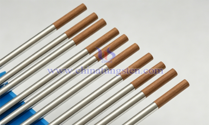
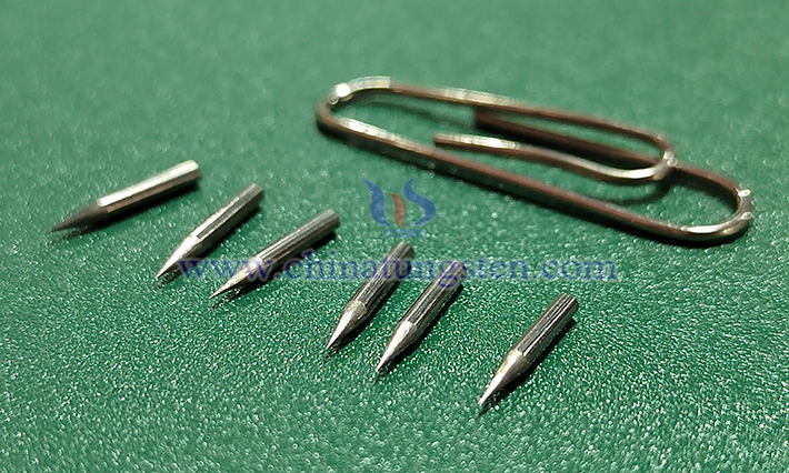
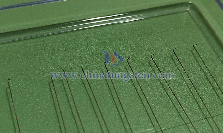
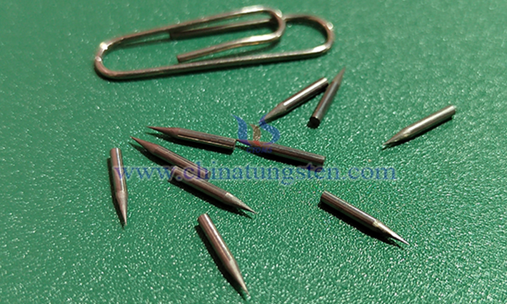
Tungsten needle produced by CTIA GROUP is a slender and sharp-pointed product made from tungsten with a purity of over 99.9% as the base material. Its main characteristics include a high melting point high hardness high density good electrical conductivity and chemical stability. These properties enable the tungsten needle to maintain stability and precision in high-temperature environments and it is widely used in industrial manufacturing electronic testing medical devices scientific research and analysis and other fields.
CTIA GROUP and its parent company, CHINATUNGSTEN ONLINE, have been dedicated to the tungsten-molybdenum products industry for nearly 30 years. They specialize in providing flexible, customized global services for tungsten-molybdenum products, designing, manufacturing, and precisely processing various standard specifications, grades, and dimensional precision according to customer requirements, suitable for a wide range of applications. For more information on tungsten electrodes, please visit the website: http://www.tungsten.com.cn/tungsten-electrodes.html. If you require tungsten electrodes, please contact CTIA GROUP: sales@chinatungsten.com, 0592-5129595.
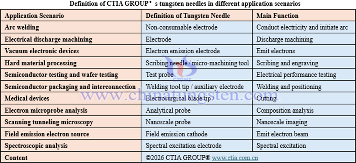
I. Applications of tungsten needles in industrial manufacturing
1.Tungsten needles for arc welding
In welding processes such as argon arc welding, tungsten needles function as non-consumable electrodes. Their main role is to conduct current and generate an electric arc, thereby melting the workpiece materials and forming a joint. The high melting point and electrical conductivity of tungsten needles enable them to maintain structural stability in high-temperature arc environments without melting or deforming. To optimize performance, rare earth oxides such as cerium oxide and lanthanum oxide are often added to the tungsten matrix. These additives improve electron emission capability, enhance arc ignition performance and arc column stability, and reduce electrode erosion rate.
In practical operation, the electrode tip geometry such as sharp angle blunt angle or beveled angle must be adjusted according to the welding area and current. In direct current electrode negative mode, the electrode tip needs to be ground into a pointed shape, and the tip angle varies with electrode diameter and welding current. For thin plate welding, small-diameter needle-like electrodes are preferred. When using alternating current, the electrode naturally forms a hemispherical tip under current action and generally does not require pre-grinding.
2.Tungsten needles in electrical discharge machining applications
In the electrical discharge machining industry, tungsten needles are defined as electrodes in EDM forming processes. Due to their high hardness, tungsten electrodes exhibit slow wear during discharge machining and are capable of replicating fine cavity structures of molds. When machining complex structures such as narrow slots and deep grooves, tungsten needles can be fabricated into slender shapes and are not prone to deformation during processing, solving the problem of bending associated with other electrode materials.
3.Tungsten needles as electron emission source materials in vacuum electronic devices
In the field of vacuum electronic devices, tungsten needles are also used as tungsten electrodes and are commonly employed as electron emission source materials. They are widely used in gas discharge tubes vacuum coating equipment and certain electron emission devices. Owing to their high melting point excellent high-temperature stability and strong electron emission capability, tungsten electrodes can achieve stable and efficient electron emission under high temperature or low pressure conditions and effectively control the discharge process, thereby forming a uniform and stable electron beam or maintaining the required discharge state.
4.Tungsten needles for hard material processing
CTIA GROUP’s tungsten needles, with high hardness and excellent wear resistance, can be used for scribing cutting or surface engraving of high-hardness materials such as metals ceramics glass and quartz. In precision machining, tungsten needles serve as micro cutting tools suitable for auxiliary processing of micro components or thin-walled structures. These operations effectively reduce material deformation and ensure high-quality machined surfaces.
II. Applications of tungsten needles in the electronics industry and semiconductor manufacturing
1.Tungsten needles for semiconductor testing probes and wafer probes
In the electronics industry, CTIA GROUP’s tungsten needles are widely used as semiconductor testing probes wafer probes and precision electrical contacts. With the development of high-density packaging and miniaturization of electronic devices, contact dimensions have reached the micrometer and even sub-micrometer scale, significantly increasing requirements for dimensional stability electrical consistency and wear life. The high rigidity of tungsten needles allows them to maintain stable deformation under small loads, preventing poor contact or excessive indentation. During frequent contact cycles, contact resistance variation remains small, typically controlled at the milliohm level, making them suitable for plug-in cycle testing scenarios. In nanoscale device testing, sub-micron tungsten needles help reduce signal noise and minimize localized electromigration risks.
In addition, in semiconductor material resistivity testing, four-probe testers often use tungsten needles as probe electrodes for electrical performance testing of semiconductor materials in factories research institutes and universities. These probes, with their excellent mechanical properties, ensure reliable test results while providing strong support for device design validation and quality control.
2.Tungsten needles for semiconductor packaging and interconnection processes
In semiconductor device processes such as gold wire bonding LED packaging and high-power electronic device contact electrode fabrication, tungsten needles are selected as welding tool tips or auxiliary positioning components due to their high melting point low evaporation rate and high-temperature dimensional stability. These applications help control welding temperature and contact points, preventing deformation or performance degradation during processing, thereby ensuring good electrical connectivity and structural integrity after packaging. This characteristic of tungsten needles is particularly suitable for micro-scale interconnection tasks and can effectively improve production efficiency and reduce defect rates.
III. Applications of tungsten needles in medical devices
In the field of medical equipment, CTIA GROUP’s tungsten needles are mainly used as consumables for electrosurgical pencil tips and minimally invasive dissection needles. The high melting point high hardness and good biocompatibility of tungsten allow the needle tips to provide sharper cutting performance than ordinary stainless steel materials. Under lower power conditions, tungsten needles enable precise cutting and coagulation while significantly reducing surgical smoke generation and minimizing thermal damage to surrounding tissues. This design allows surgeons to better protect patient tissues while ensuring therapeutic outcomes and avoiding unnecessary side effects. Medical tungsten needles are widely used in general surgery neurosurgery oral surgery plastic surgery and cardiothoracic surgery.
IV. Applications of tungsten needles in scientific research and analytical instruments
1.Tungsten needles for electron microprobe analysis
Tungsten needles are commonly used probe materials in electron microprobe analysis. This instrument combines electron beam and X-ray spectroscopy technologies to perform qualitative and quantitative analysis of alloy microstructures mineral compositions and more. Due to their high melting point and thermal resistance, tungsten needles can withstand relatively high current density and energy density at elevated temperatures, helping maintain probe sensitivity and stability. This performance advantage makes tungsten needles highly reliable in complex microstructural characterization and widely used in materials science and geological research.
2.Tungsten needles for scanning tunneling microscopy and atomic force microscopy probes
Tungsten needles sharpened to nanometer-scale tip radii by electrochemical etching are commonly used as probes in scanning tunneling microscopy, where tunneling current between the tip and sample surface is used to analyze atomic surface structures. In atomic force microscopy, tungsten needles can also serve as support cantilevers or conductive probes. These nanoscale probes enable high-resolution three-dimensional surface imaging, providing powerful tools for nanomaterials biomolecules and device defect analysis, improving research efficiency and data accuracy.
3.Tungsten needles for field emission electron sources
In field emission scanning electron microscopes, CTIA GROUP’s tungsten needles can be sharpened at the tip and used as field emission electron sources to generate high-energy electron beams for surface imaging. In some cathode ray tubes and field emission displays, tungsten needles have also been used as cathode materials or emission tips. These applications require excellent electron emission performance and thermal stability, enabling continuous stable and focused electron flow in high-vacuum environments, providing critical support for high-resolution imaging and display technologies.
4.Tungsten needles in spectroscopic analysis applications
In spectroscopic analysis laboratories, tungsten needles are defined as stable spectral excitation electrodes. Under arc excitation at specific currents, tungsten needles generate continuous spectra covering ultraviolet to visible wavelengths, providing a stable light source for quantitative analysis of metallic elements. By optimizing the tip grinding angle, spectral focusing performance can be improved and radiation intensity fluctuations can be minimized. In scenarios such as environmental monitoring and heavy metal detection in food, where high data accuracy is required, the stable spectra provided by tungsten needles reduce analytical errors, improving reliability of results and supporting environmental management and food safety control.